

Global Vacuum Radio Frequency (RF) Sputtering Coating Equipment Market to Reach USD 555 Million by 2032, Growing at a CAGR of 4.9%

MARKET INSIGHTS
Global Vacuum Radio Frequency (RF) Sputtering Coating Equipment market size was valued at USD 399 million in 2024 and is projected to grow from USD 418 million in 2025 to USD 555 million by 2032, exhibiting a CAGR of 4.9% during the forecast period.
Report Sample includes:
- Table of Contents
- List of Tables & Figures
- Charts
- Research Methodology
Get FREE Sample of this Report at https://www.intelmarketresearch.com/download-free-sample/3147/vacuum-radio-frequency-sputtering-coating-equipment-market
Vacuum RF Sputtering Coating Equipment is a precision deposition system that utilizes radio-frequency power to create thin films in a vacuum environment. The technology generates an alternating electric field that ionizes inert gases, causing them to bombard target materials and deposit atoms onto substrates with high uniformity. This equipment is critical for producing coatings with superior adhesion, density, and microstructural control compared to conventional methods.
The market growth is driven by increasing demand from semiconductor manufacturing and photovoltaic applications, where precise thin-film deposition is essential. While North America currently leads in technological adoption, Asia-Pacific shows the fastest growth due to expanding electronics production capacities. Key manufacturers like Applied Materials (AMAT) and Plasma Process Group are investing in advanced multi-target systems to cater to emerging requirements in optoelectronics and flexible electronics. The Single Target RF Sputtering Equipment segment accounted for over 60% of 2024 revenue, though multi-target systems are gaining traction for complex coating applications.
MARKET DYNAMICS
MARKET DRIVERS
Expanding Semiconductor Industry Accelerates Demand for RF Sputtering Equipment
The global semiconductor market, valued at over $600 billion in 2024, continues to drive significant demand for vacuum RF sputtering equipment. As chip manufacturers push for smaller node sizes below 5nm, the need for precise thin-film deposition has become critical. RF sputtering enables uniform coating of dielectric materials essential for advanced semiconductor fabrication, offering superior step coverage compared to DC sputtering. Major semiconductor foundries are investing heavily in expanding production capacity, with spending on wafer fabrication equipment projected to grow at 7-9% annually through 2026. This sustained capital expenditure creates a robust market for high-performance sputtering systems capable of meeting strict purity and uniformity requirements.
Rising Adoption in Photovoltaic Manufacturing Boosts Market Growth
The solar energy sector continues to be a key driver for RF sputtering equipment, particularly for manufacturing thin-film photovoltaic cells. With global solar installations expected to surpass 350 GW annually by 2025, manufacturers are increasingly turning to RF sputtering for depositing transparent conductive oxide (TCO) layers and other functional coatings. This technology enables precise control over film properties critical for solar cell efficiency, such as conductivity and light transmittance. The market for photovoltaic sputtering equipment is further propelled by growing investments in next-generation perovskite solar cells, which require multiple precisely tuned layers that RF sputtering can effectively deposit.
Technological Advancements Enhance Equipment Capabilities
Recent innovations in RF sputtering technology are expanding its applications across industries. Advanced power delivery systems now enable more stable plasma conditions, reducing arcing and improving film quality. Next-generation magnetron designs achieve higher target utilization rates exceeding 50%, significantly lowering operational costs. The integration of real-time process monitoring and AI-driven control systems allows for unprecedented precision in film thickness and composition. These technological improvements make RF sputtering increasingly attractive for demanding applications such as micro-electromechanical systems (MEMS) and advanced optical coatings, where nanometer-scale uniformity is crucial.
MARKET RESTRAINTS
Sponsored
Sponsored
Categories
- AI
- Design
- Fashion and Art
- Investment and Finance
- Top 10
- Christianity
- Climate and Enviroment
- Writing and Film
- Fitness
- Food
- Games
- Gardening
- Health
- Home and Interiors
- Marketing and Sales
- Music
- Making Money Online
- Others
- Books
- Religion
- Ecommerce
- Sports
- Cars
- Wellness
- Tech Gadgets
- Events
- Governments and Nations
- Science and Engineering
- Real Estate
- Travel, Tourism and Hospitality
- Education
- Startups
- Beauty and Cosmetics
- Agriculture
- Computer Operating Systems
- Crypto
- Politics and News
- Video Review
- Immigration
Read More
Competitive Analysis of Executive Summary Tankless Water Heater Market Size and Share Tankless water heater market is expected to grow at a compound annual growth rate of 5.62% in the forecast period of 2021 to 2028. Global Tankless Water Heater Market report comprises of data that can be quite essential when it comes to dominate the market or making a mark in the market as a new...
Executive Summary: Facial Recognition Market Size and Share by Application & Industry CAGR Value: The global facial recognition market size was valued at approximately USD 5.2 billion in 2024 and is projected to reach USD 8.3 billion by 2032, growing at a CAGR of 7.0% during the forecast period (2024–2032). For the growth of...

I have gotten five piercings at four lobe piercings and one cartilage. everyone warned me before I got my cartilage pierced at the age of to get my cartilage pierced with a, but I was terrified of needles and really wanted a cartilage piercing. The only people willing to do it with a piercing were the brave employees at., the piercing only lasted a year longer than I expected, honestly, it kept...

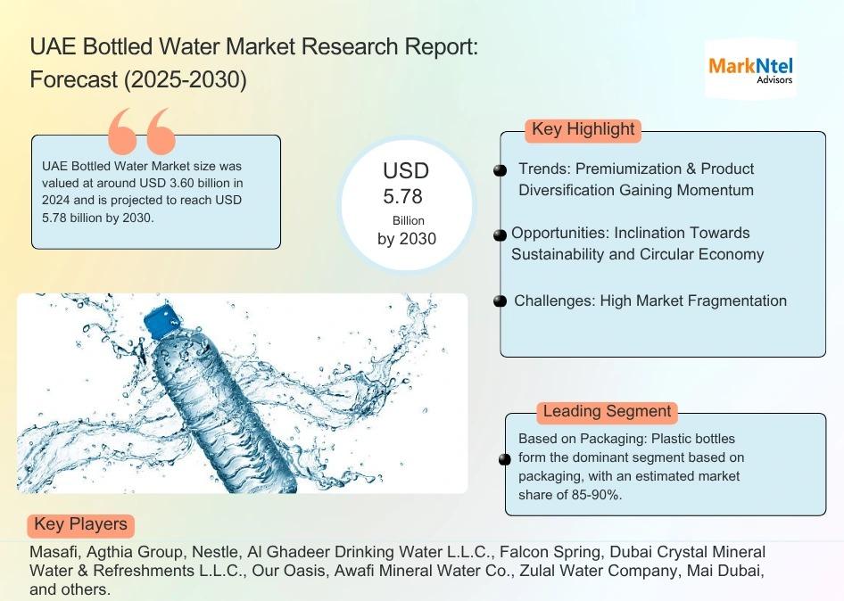
MarkNtel Advisors, a leading market research and consulting firm, has announced the release of its latest study titled UAE Bottled Water Market Research Report: Forecast (2025–2030). This report provides a detailed assessment of the UAE Bottled Water, covering its evolving dynamics, emerging trends, key growth drivers, major challenges, and competitive landscape. Designed to guide...
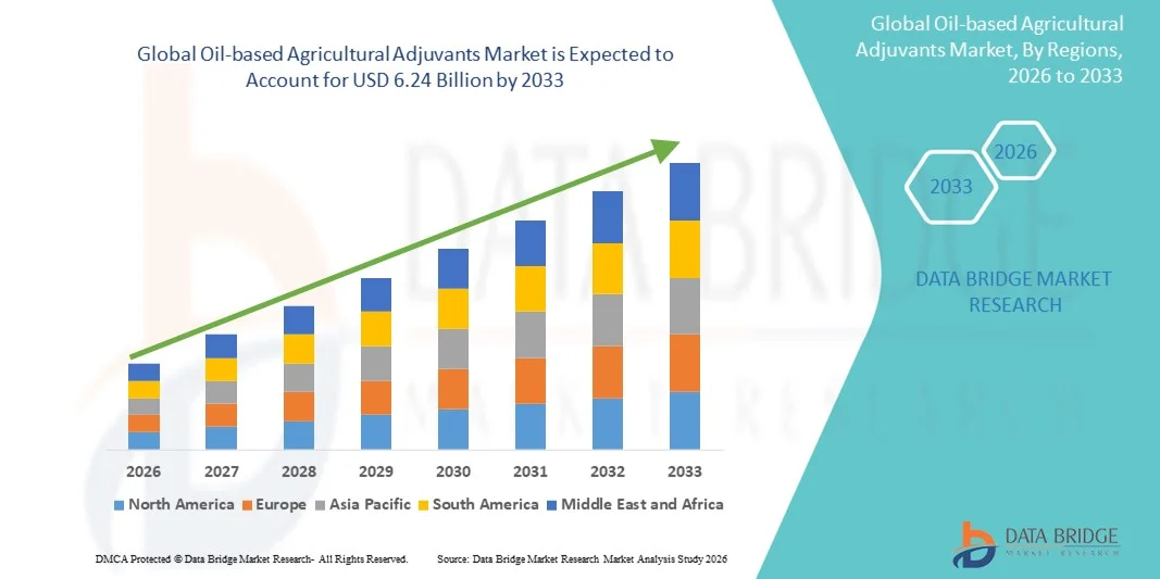
The global Oil-based Agricultural Adjuvants Market is currently experiencing a sustained period of capital intensification and technological refinement as growers prioritize input efficiency over volume. The global Oil-based Agricultural Adjuvants Market size was valued at USD 4.19 billion in 2025 and is expected to reach USD 6.24 billion by 2033, at a CAGR of...